PIC18F4550 microcontroller has 1 CCP (Capture/Compare/PWM) module which is CCP2 module and 1 ECCP (Enhanced CCP) module which is CCP1 module.
This topic shows how to use CCP and ECCP modules as PWM modules.
The ECCP module can work as a standard CCP module or ECCP module.
Timer2 is used in the determination of the PWM frequency.
PWM Period:
The PWM period is specified by writing to the PR2 register. The PWM period can be calculated using the following formula:
PWM period = [(PR2) + 1] • 4 • Tosc • (TMR2 Prescale Value)
And the PWM frequency is defined as 1/[PWM period].
For example for PR2 = 250 , microcontroller frequency = 8MHz and Prescale = 16 we get a PWM frequency of 500Hz.
The CCS Timer2 configuration has the following form:
setup_timer_2(mode, period, postscale);
where: mode is TMR2 Prescale Value, period is PR2 and postscaler is not used in the determination of the PWM frequency (keep it 1).
Previous example gives the following Timer2 configuration command:
setup_timer_2(T2_DIV_BY_16, 250, 1);
PWM Duty Cycle:
PIC18F4550 has a maximum PWM duty cycle of 10-bit and for CCS C compiler the following two lines are used to write PWM1 and PWM2 duty cycles respectively:
set_pwm1_duty (value);
set_pwm2_duty (value);
Where ‘value’ may be an 8 or 16 bit constant or variable.
The 10 bit value is then used to determine the duty cycle of the PWM signal as follows:
duty cycle = value / [ 4 * (PR2 +1 ) ]
For the previous example where PR2 = 250:
Minimm duty cycle = 0 ===> value = 0.
Maximum duty cycle = 1 (100%) ===> value = 1004.
If value is greater than 1004 PWM1 output or PWM2 output will not be cleared.
For this example PWM duty cycle range is between 0 and 1023.
If an 8-bit value is used, the duty cycle of the PWM signal is determined as follows:
duty cycle=value/(PR2+1)
For the previous example where PR2 = 250:
Minimum duty cycle = 0 ===> value = 0.
Maximum duty cycle = 1 (100%) ===> value = 251.
If we want to get 1KHz PWM frequency with 8MHz mcu frequency then Timer2 configuration is:
setup_timer_2(T2_DIV_BY_16, 124, 1);
For maximum resolution:
Minimum duty cycle = 0 ===> value = 0.
Maximum duty cycle = 1 (100%) ===> value = 500.
Here maximum duty cycle resolution is a little bit less than 9-bit and duty cycle range is from 0 to 511.
For values from 500 and 511 PWMs outputs will not be cleared and duty cycle value shouldn’t exceed 511.
If you want to stop the PWM signal use the following two commands for PWM1 and PWM2 respectively:
setup_ccp1(CCP_OFF);
setup_ccp2(CCP_OFF);
Standard PWM mode:
In standard mode ECCP works as simple PWM module and a PWM signal is produced on pin RC2. The CCP2 module produces a PWM signal on pin RC1.
In CCS C compiler the following lines configures the CCP modules as PWM modules:
setup_ccp1(CCP_PWM); // Configure CCP1 as a PWM
setup_ccp2(CCP_PWM); // Configure CCP2 as a PWM
PIC18F4550 standard PWM example with CCS C:
This is a simple example shows how to use ECCP (CCP1) and CCP2. Circuit schematic is shown below.
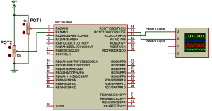 In the above circuit there are 2 potentiometers POT1 and POT2. These pots are used to set PWM1 and PWM2 duty cycles respectively. PWM1 output (RC2) and PWM2 output (RC1) are connected to an oscilloscope channels A and B.
PIC18F4550 microcontroller internal oscillator is used @ 8MHz and MCLR pin function is disabled.
PIC18F4550 PWM1 and PWM2 example CCS C code:
1 2 3 4 5 6 7 8 9 10 11 12 13 14 15 16 17 18 19 20 21 22 23 24 25 26 27 28 29 | // PIC18F4550 standard PWM example CCS C code #include <18F4550.h> #device ADC = 10 #fuses NOMCLR INTRC_IO #use delay(clock = 8000000) unsigned int16 i, j ; void main(){ setup_oscillator(OSC_8MHZ); // Set internal oscillator to 8MHz setup_adc(ADC_CLOCK_DIV_8); // Set ADC conversion time to 8Tosc setup_adc_ports(AN0_TO_AN1); // Configure AN0 & AN1 as analog inputs setup_ccp1(CCP_PWM); // Configure CCP1 as standard PWM setup_ccp2(CCP_PWM); // Configure CCP2 as standard PWM setup_timer_2(T2_DIV_BY_16, 250, 1); // Set PWM frequency to 500Hz delay_ms(100); // Wait 100ms while(TRUE){ set_adc_channel(0); // Select channel AN0 delay_ms(1); // Wait 1ms i = read_adc(); // Read from AN0 and store in i delay_ms(1); // Wait 1ms set_adc_channel(1); // Select channel AN1 delay_ms(1); // Wait 1ms j = read_adc(); // Read from AN1 and store in j set_pwm1_duty(i); // Set pwm1 duty cycle to i set_pwm2_duty(j); // Set pwm2 duty cycle to j delay_ms(1); // Wait 1ms } } |
PIC18F4550 PWM1 and PWM2 example video:
The following video shows example simulation using Proteus.
Enhanced PWM mode:
The Enhanced PWM mode provides additional PWM output options for a broader range of control applications. The module is a backward compatible version of the standard CCP module and offers up to four outputs, designated P1A through P1D. Users are also able to select the polarity of the signal (either active-high or active-low).The enhanced PWM can work in different modes:
Half-Bridge Output
Full-Bridge Output, Forward mode
Full-Bridge Output, Reverse mode
Half-Bridge mode:
In the Half-Bridge Output mode, two pins are used as outputs to drive push-pull loads. The PWM output signal is output on the P1A pin (pin 17), while the complementary PWM output signal is output on the P1B pin (pin 28) (see the following figure with output signals are shown as active high).
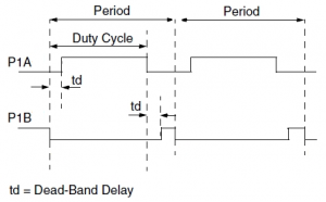 In Half-Bridge Output mode, the programmable dead-band delay can be used to prevent shoot-through current in half-bridge power devices.
In CCS C compiler, to setup the enhanced CCP module as Half-Bridge output mode use the following command:
setup_ccp1(CCP_PWM | CCP_PWM_HALF_BRIDGE);
And to stop the PWM output use the following command:
setup_ccp1(CCP_OFF);
PIC18F4550 EPWM half-bridge mode example:
This example shows how to use the enhanced PWM as half-bridge output mode. Circuit schematic is shown below.
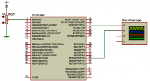 POT is used to change the PWM duty cycle.
PIC18F4550 internal oscillator is used and MCLR pin function is disabled.
PIC18F4550 Half-Bridge output mode example CCS C code:
1 2 3 4 5 6 7 8 9 10 11 12 13 14 15 16 17 18 19 20 21 22 | // PIC18F4550 Half-Bridge mode EPWM example CCS C code #include <18F4550.h> #device ADC = 10 #fuses NOMCLR INTRC_IO #use delay(clock = 8000000) unsigned int16 i ; void main(){ setup_oscillator(OSC_8MHZ); // Set internal oscillator to 8MHz setup_adc(ADC_CLOCK_DIV_8); // Set ADC conversion time to 8Tosc setup_adc_ports(AN0); // Configure AN0 as analog input set_adc_channel(0); // Select channel AN0 setup_timer_2(T2_DIV_BY_16, 250, 1); // Set PWM frequency to 500Hz setup_ccp1(CCP_PWM | CCP_PWM_HALF_BRIDGE); delay_ms(100); // Wait 100ms while(TRUE){ i = read_adc(); // Read from AN0 and store in i set_pwm1_duty(i); // Set pwm1 duty cycle to i delay_ms(1); // Wait 1ms } } |
PIC18F4550 Half-Bridge PWM mode example simulation video:
Full Bridge PWM mode:
In Full-Bridge Output mode, four pins are used as outputs; however, only two outputs are active at a time. In the Forward mode, pin P1A is continuously active and pin P1D is modulated. In the Reverse mode, pin P1C is continuously active and pin P1B is modulated.
Output signals shown as active-high.
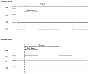 CCS C commands for forward mode and reverse mode are as below respectively: setup_ccp1(CCP_PWM | CCP_PWM_FULL_BRIDGE);
setup_ccp1(CCP_PWM | CCP_PWM_FULL_BRIDGE_REV);
PIC18F4550 Enhanced PWM Full-Bridge mode example:
Here is a simple example shows how to start with PIC18F4550 microcontroller full-bridge PWM mode, circuit schematic is shown below.
 The potentiometer is used to set the PWM duty cycle and the pushbutton to toggle between the forward and reverse modes.
PIC18F4550 Enhanced PWM Full-Bridge mode example CCS C code:
1 2 3 4 5 6 7 8 9 10 11 12 13 14 15 16 17 18 19 20 21 22 23 24 25 26 27 28 29 30 | // PIC18F4550 Full-Bridge mode EPWM example CCS C code #include <18F4550.h> #device ADC = 10 #fuses NOMCLR INTRC_IO #use delay(clock = 8000000) short mode; unsigned int16 i ; void main(){ setup_oscillator(OSC_8MHZ); // Set internal oscillator to 8MHz setup_adc(ADC_CLOCK_DIV_8); // Set ADC conversion time to 8Tosc setup_adc_ports(AN0); // Configure AN0 as analog input set_adc_channel(0); // Select channel AN0 setup_timer_2(T2_DIV_BY_16, 250, 1); // Set PWM frequency to 500Hz delay_ms(100); // Wait 100ms while(TRUE){ if(input(PIN_B0) == 0){ mode = ~mode; // Toggle mode variable if(mode == 1) setup_ccp1(CCP_PWM | CCP_PWM_FULL_BRIDGE); // Forward output mode else setup_ccp1(CCP_PWM | CCP_PWM_FULL_BRIDGE_REV); // Reverse output mode delay_ms(500); } i = read_adc(); // Read from AN0 and store in i set_pwm1_duty(i); // Set pwm1 duty cycle to i delay_ms(1); // Wait 1ms } } |
PIC18F4550 Full-Bridge PWM mode simulation video:
For the enhanced CCP some other commands can be used to determine the active state of the outputs (active high or active low), these commands must be OR’ed with the previous command using the character | .
The default command is the first one.
CCP_PWM_H_H //P1A, P1C active-high; P1B, P1D active-high
CCP_PWM_H_L //P1A, P1C active-high; P1B, P1D active-low
CCP_PWM_L_H //P1A, P1C active-low; P1B, P1D active-high
CCP_PWM_L_L //P1A, P1C active-low; P1B, P1D active-low
Example:
setup_ccp1(CCP_PWM | CCP_PWM_FULL_BRIDGE | CCP_PWM_H_L);
Reference:
Microchip PIC18F4550 datasheet.
Discover more from Simple Circuit
Subscribe to get the latest posts sent to your email.
