This post shows the design of a low cost precision analog isolation amplifier using HCNR201 (HCNR200) optocoupler where input signal is galvanically isolated from output signal.
The HCNR201/HCNR200 can be used to isolate analog signals in a wide variety of applications that require good stability, linearity, bandwidth, and low cost.
About The HCNR201 Optocoupler:
The HCNR201 (HCNR200) optocoupler from Broadcom is a high-linearity analog optocoupler consists of a high-performance AlGaAs LED that illuminates two closely matched photodiodes. The input photodiode can be used to monitor, and therefore stabilize, the light output of the LED. As a result, the nonlinearity and drift characteristics of the LED can be virtually eliminated. The output photodiode produces a photocurrent that is linearly related to the light output of the LED. The close matching of the photodiode and advanced design of the package ensure the high linearity and stable gain characteristics of the optocoupler.
The HCNR201 can be used to isolate analog signals in a wide variety of applications that require good stability, linearity, bandwidth and low cost. The HCNR201 is very flexible and, by appropriate design of the application circuit, is capable of operating in many different modes, including: unipolar/bipolar, AC/DC and inverting/non-inverting. The HCNR201 is an excellent solution for many analog isolation problems.
HCNR200/201 Schematic:
The HCNR200 (HCNR201) optocoupler is just an 8-pin integrated circuit comes in 8-pin DIP or 8-pin Gull Wing package. A general schematic is shown below:
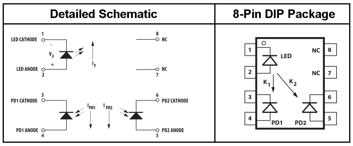
Operation of the HCNR200/HCNR201 optocoupler:
The HCNR200/HCNR201 consists of a high-performance AlGaAs LED emitter coupled to two totally independent photodiodes. As shown in the schematic above, the internal LED pins are 1 & 2 respectively for cathode & anode terminals, photodiode PD1 (pins 3 & 4), and photodiode PD2 (pins 5 & 6). PD1 and PD2 currents, IPD1 and IPD2 are directly proportional to the LED light intensity.
The photodiode PD1 is located in the input side of the photocoupler and it is generally used as a servo photodiode which provides a feedback signal to the LED and therefor the ability to control the current that flows through it. The second photodiode PD2 is located in the output side of the optocoupler, it is galvanically isolated and independent from PD1.
Input photodiode PD1 current transfer ratio, K1:
The input photodiode PD1 current transfer ratio (also known as servo gain) is defined as the ratio of PD1 output current IPD1 and the dive LED current IF.
K1 = IPD1/IF
As written in device datasheet, the HCNR200 has a typical K1 of 0.5%, and the HCNR201 has a typical K1 of 0.48%. As an example, for the HCNR201 and for an LED current IF of 10mA the typical PD1 current is 48uA.
Output photodiode PD2 current transfer ratio, K2:
The output photodiode PD2 current transfer ratio (also known as output forward gain) is defined as the ratio of PD2 output current IPD2 and the dive LED current IF.
K2 = IPD2/IF
Transfer gain, K3:
Transfer gain (also known as Current Transfer Ratio, CTR) is an important parameter that describes the performance of the optocoupler. It is defined as the ratio of PD2 current transfer ratio and PD1 current transfer ration, or simply:
K3 = K2/K1
The datasheet of the device gives a typical K3 value of 1.00 with a tolerance of ±15% for the HCNR200 and ±5% for the HCNR201.
Note that HCNR200 differs from HCNR201 in some parameters, the pinout of the two devices are the same, datasheet contains more information including electrical parameters of each device.
Applications of the HCNR200/HCNR201 Optocoupler:
- Low cost analog isolation
- Telecom: Modem, PBX
- Industrial process control: Transducer isolator
- Isolator for thermocouples 4 mA to 20 mA loop isolation
- SMPS feedback loop, SMPS feedforward
- Monitor motor supply voltage
- Medical
Isolation amplifier using HCNR200/HCNR201 optocoupler:
An isolation amplifier is an amplifier with an output separated from the input circuitry, in other words, the output side of the isolation amplifier has no direct contact with the input side including the power supply circuit.
Today there are many single-chip isolation amplifiers. These chips are easy to use and small in size which saves space, but they are expensive. Some types of isolation amplifiers are: AMC1301 from Texas Instruments and APL-C78A from BROADCOM.
Applications of the isolation amplifier:
- General purpose AC & DC voltage and current sensing
- Switched mode power supply signal isolation
- General purpose analog signal isolation
The HCNR201 (HCNR200) optocoupler can be used to build a low cost precision isolation amplifier. Circuit diagram is shown below.
Note that there are some alternatives to the HCNR201 optocoupler, for example IL300 from Vishay and LOC110 (or LOC111) from IXYS. Using an alternative may require different values for some resistors used in the circuit.
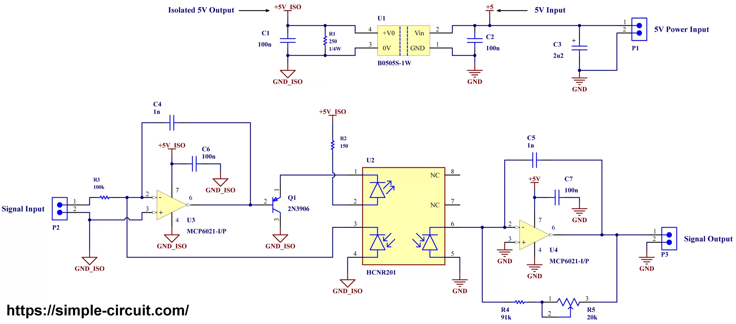
Hardware Required:
- HCNR201 (or HCNR200) optocoupler (U2) —> datasheet
- B0505-1W Isolated DC/DC converter (U1) —> datasheet
- 2 x MCP6021-I/P operational amplifier (U3, U4) —> datasheet
- 2N3906 PNP transistor (Q1)
- 250 ohm, 1/4 W resistor (R1)
- 150 ohm resistor (R2)
- 100k ohm resistor (R3)
- 91k ohm resistor (R4)
- 20k ohm variable resistor (R5), type: 3296W-1-203
- 16V, 2u2 electrolytic capacitor (C3)
- 4 x 100n ceramic capacitor (C1, C2, C6, C7)
- 2 x 1n ceramic capacitor (C4, C5)
- 3 x two position connectors (P1, P2, P3)
The MCP6021-I/¨P is an operational amplifier from Microchip, it is 8-pin low cost integrated circuit.
Other standard op amps can be used in the circuit instead of the MCP6021 (U3 & U4), for example LM158
Circuit Description:
The HCNR201 consists of main LED and photodiode PD1 on the input side, and photodiode PD2 on the output side, pins 7 and 8 are not connected pins. The package of the optocoupler HCNR201 is constructed so that each photodiode receives approximately the same amount of light from the LED.
In the circuit there are 3 separated terminal block connectors each with 2 positions, the first one labeled as P1 is circuit power supply terminal with 5V input. The second terminal is P2 and it is for signal input (signal needs to be isolated). The last terminal block is P3 and is for signal output.
Signal Input Circuit:
An operational amplifier (OP AMP) labeled as U3 is used with PD1 optocoupler to sense light intensity output from the optocoupler’s LED and automatically adjusts the current that flows through the LED with the help of Q1 transistor (2N3906 PNP transistor). A resistor of 150 ohm (R2) is used to limit the current flowing through the LED.
As the non-inverting input (+) of op amp U3 is connected to the ground (GND_ISO) the op amp will try to maintain its inverting input (-) at zero volt also (with respect to GND_ISO), this can be achieved by increasing the current flowing through optocoupler’s LED and therefor increasing photodiode PD1 current.
The property of high input impedance of the operational amplifier keeps the photodiode PD1 current equal (theoretically) to the current that passes through resistor R3.
If the input signal voltage increased, the voltage of the inverting input of U3 also will increase, the inverting input voltage becomes higher than the voltage of the non-inverting input, here the U3 op amp outputs 0V.
The transistor Q1 (2N3906) is PNP type, its base terminal is directly connected to the output of U3 op amp. This means Q1 transistor is driven by U3 op amp and the current that flows from the emitter to the collector of Q3 depends on the output voltage of U3. If the output voltage of U3 is zero (with respect to GND_ISO) then the current flowing through the optocoupler’s LED is approximately:
IF = (5 – VF)/R2 = (5 – 1.6)/150 = 22.67 mA
where VF is the forward voltage of the LED (typical value).
As the output of U3 op amp is zero a current of 22.67 mA will start flowing through HCNR200/HCNR201 optocoupler’s LED and photodiodes PD1 & PD2 start generating current (in uA). With a current starts flowing through PD1 photodiode (and also resistor R3) the output voltage of U3 op amp begins to increase until PD1 current is sufficient to make the inverting input voltage and non-inverting input voltage equal, thus, current flows through PD1 photodiode IPD1 can be expressed as:
IPD1 = Vin/R3
where Vin is the input signal voltage
Power circuit:
To satisfy the isolation property between the input signal and the output signal, the input signal power supply must also be isolated from the output signal power supply. For this purpose I used an isolated DC-to-DC converter which annotated in the circuit schematic as U1. In this project I used MORNSUN B0505-1W low cost unregulated DC/DC converter with 5V input and 5V output, other equivalents such as RECOM RFM-0505S (–datasheet–) can be used. Using an isolated DC/DC converter provides a galvanic isolation between the input voltage and the output voltage.
The input power supply voltage of the circuit is 5V, connector P1 is used for the power supply connection where terminal #1 is power supply positive input (+5V) and #2 is negative input (GND). The isolated 5V source comes from the isolated DC/DC converter (U1) with +5V_ISO is positive and GND_ISO is negative. Note that there is no direct physical connection between GND and GND_ISO.
Signal Output Circuit:
In the circuit output side there is another op amp annotated as U4, this op amp with resistor R4 and variable resistor R5 are used to convert photodiode PD2 current into voltage. The variable resistor R5 is mainly used to calibrate the circuit.
The current produced by PD2 and passing through resistors R4 & R5 generates a negative voltage at the inverting input of U4 operational amplifier, this causes the op amp to raise its output voltage until the inverting input voltage equals to the non-inverting input voltage which is directly connected to the ground (GND).
The combination of photodiode PD1, U4 operational amplifier, and feedback resistor (R4 + R5) works as a Transimpedance Amplifier (TIA) which is simply a current to voltage converter, the current source is the photodiode PD2.
The output voltage VOUT can be expressed as:
VOUT = IPD2 x (R4 + R5)
so
VOUT/IPD2 = (R4 + R5)
therefor the gain of this Transimpedance Amplifier (TIA) is the feedback resistor value (R4 + R5).
Optocoupler transfer gain (photodiode current ratio) K3:
K3 = K2/K1 = IPD2/IPD1
Combining previous equations gives a relation between input voltage and output voltage:
VOUT/VIN = K3 x (R4 + R5) / R3
Therefore the relationship between VIN and VOUT is constant, linear, and independent of the light output characteristics of the LED.
Assume K3 = 1 and R3 = R4 + R5, previous equation gives that the input voltage equals the output voltage:
VOUT = VIN
In our circuit the variable resistor R5 of 20k is set so that the voltage of the input signal is equal to the voltage of the output signal, this yields a gain equal to 1.
The feedback capacitors C4 & C5 respectively for U3 & U4 op amps, each of capacitance of 1 nanofarad, are used to improve circuit stability, they also reduce the bandwidth of the circuit. The bandwidth of the circuit can be calculated using this function:
f = 1/(2π x R x C)
where R is the feedback resistor and C is the feedback capacitor.
In our circuit the feedback resistor is 100k and the feedback capacitor is 1nF, the photodiode capacitance and the op amp input capacitance can be neglected with respect to the feedback capacitance, so the frequency response is:
f = 1/(2π x 100k x 1n) = 1591 Hz
Isolation amplifier with HCNR201 optocoupler test circuit:
I built a DIY circuit for testing purpose of this project, I used a variable DC voltage source for the input signal (signal to be isolated). To clearly watch the variation of the output signal voltage with respect to the input signal voltage, I connected a digital multimeter at the input signal connection terminals and another digital multimeter at the output signal terminals.
The video below shows the test circuit:
Reference:
Broadcom HCNR200 and HCNR201 High-Linearity Analog Optocouplers Datasheet
Discover more from Simple Circuit
Subscribe to get the latest posts sent to your email.
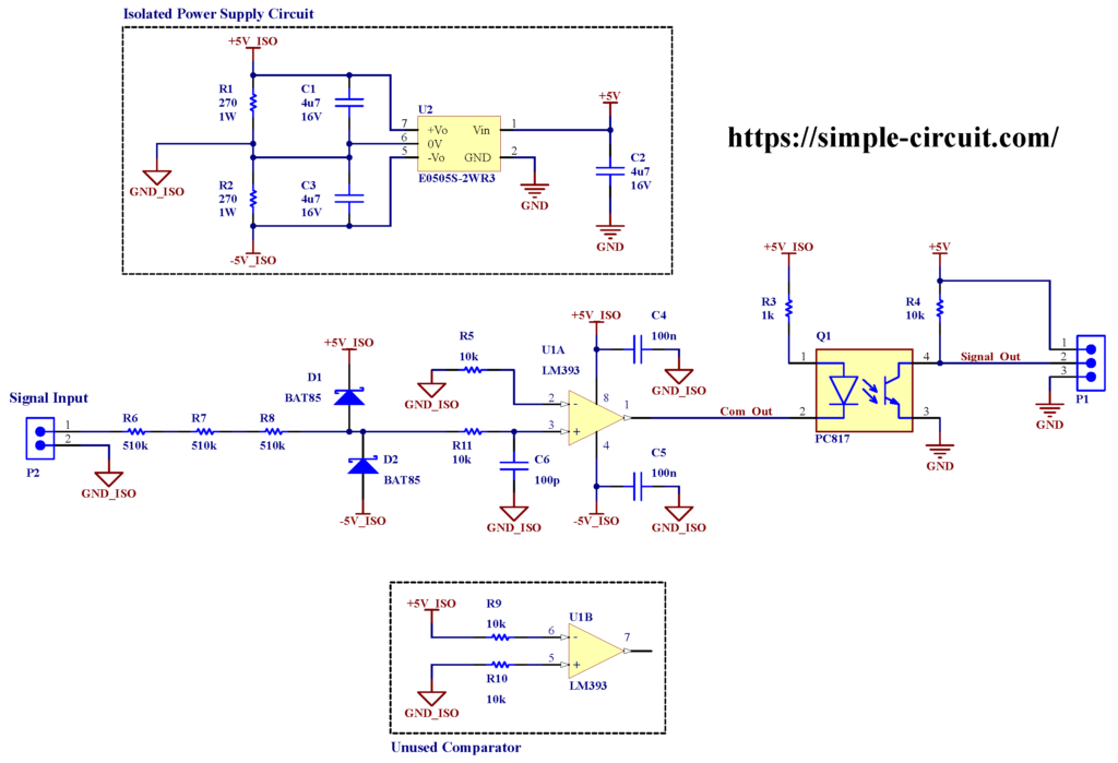
Isolated 1-5V to 0-10V Converter
Is it possible?
You may prefer to use isolated 5V and isolated GND on the output side as that is usually the environment that contains noise. What is your opinion about it?
Generally the input signal comes from a hazardous environment for example high voltage whereas the output signal goes to a low voltage circuit such as a microcontroller which may be connected to a PC or get in direct contact with human body. The isolation name here when applied to the input signal circuitry will be more correct.
Isolated 0-5V to 0-10V Converter
The applied voltage is 24V single power supply.
Output 0V fine adjustment variable resistance (Zero)
Output 10V fine adjustment variable resistor (SPAN)
Application Circuit ~~?
You need to change some resistor values, R3 in the input side and R4 & R5 in the output side.
Resistor values can be easily obtained using the equations mentioned above, here you have VOUT/VIN = 2.