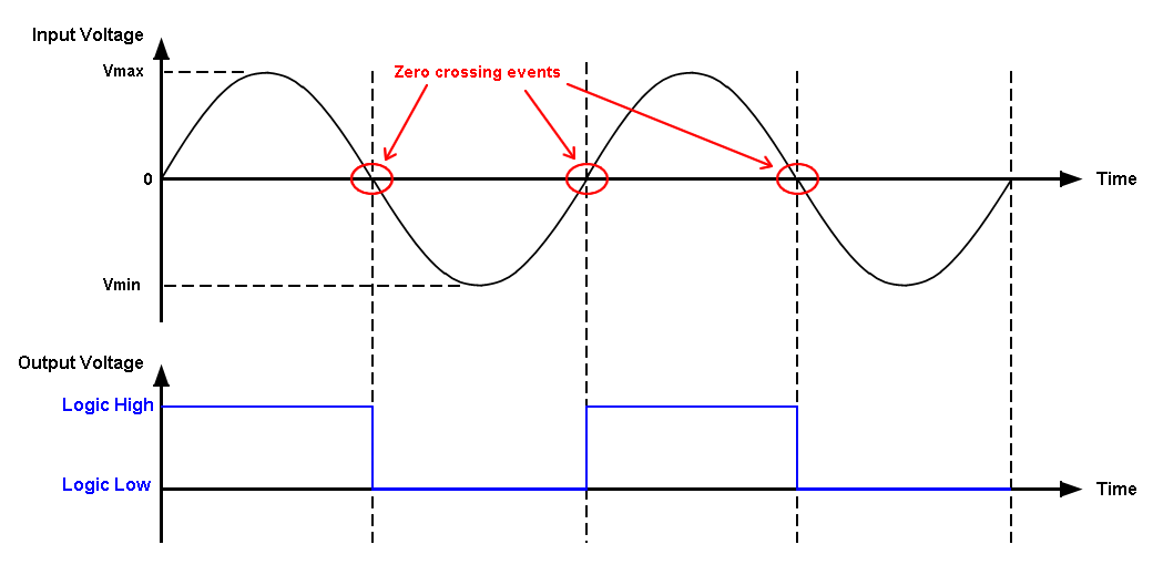
A zero crossing detector is an electronic circuit used to detect the exact moment when the voltage of an alternating current (AC) signal passes through zero volts. In other words, the zero-crossing detection circuit detects when an AC signal voltage changes from positive to negative and vice versa.
Basically, the zero-crossing detector circuit has an analog input for the AC signal and a logic output that changes with respect to the input AC signal. For example if the input signal is in its positive cycle then the circuit outputs a logic high (or logic low depending on the design of the circuit), and if the input signal is in its negative cycle then the circuit outputs a logic low (or logic high).
The following image shows the input voltage waveform (AC sinewave) and the corresponding output of a zero-crossing detector circuit:
Zero-Crossing Detection Circuit Applications:
These are some applications where zero crossing detector circuit is used.
One of the primary applications of zero crossing detection circuits is in power control systems where zero crossing events are synchronized with the switching of power electronic devices such as thyristors (SCR), TRIACs, or MOSFETs, to control the flow of electric current.
The zero-crossing detection circuit is used also in motor control applications. For example controlling a sensorless brushless DC motor (BLDC Motor) requires the knowledge of its rotor position, this can be achieved by sensing the zero crossing events of the back-emf (Electromotive Force) generated by the rotor.
Zero crossing detection circuits are widely used in lighting applications, the light dimmer mainly consists of a power triac or thyristor used to control the current flowing through the lamp. The power device switching is synchronized with the events when the input AC voltage crosses the zero points.
Working Principle of a Zero Crossing Detection Circuit:
It is easy to know the polarity of a signal, whether it is positive or negative. This is can be done using a comparator or an operational amplifier (op-amp) circuit. If the output of the comparator (or the op-amp when used as comparator) state changed means that the input voltage polarity was also changed. The moment of change of comparator’s output is when the input signal crosses the zero point.
The following image shows a basic circuit diagram of a zero crossing detector using comparator.
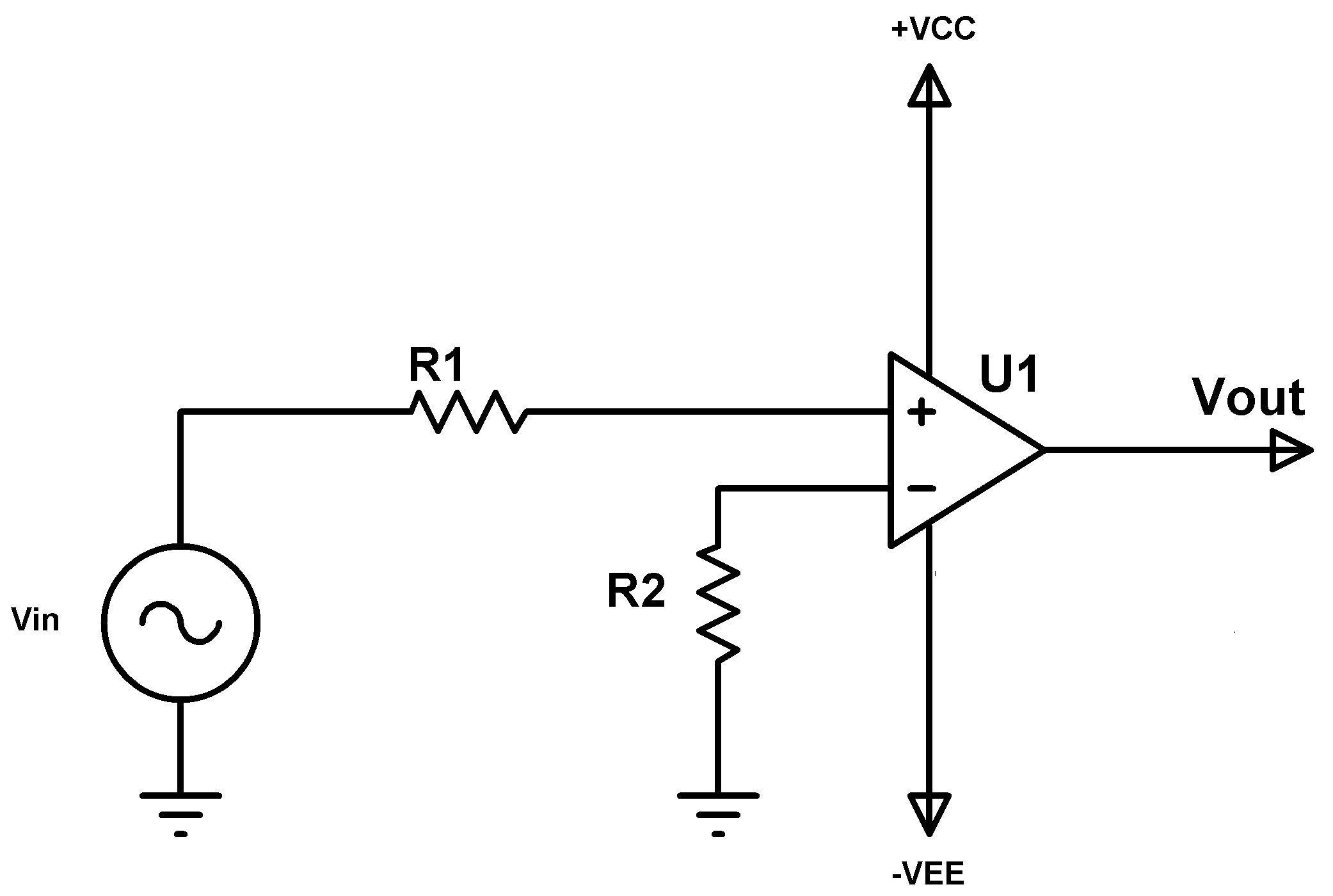
The main component of this circuit is the analog differential comparator (U1). A dual supply is used to power the analog comparator with +VCC is the positive and -VEE is the negative, both with respect to circuit ground (GND).
The input voltage is sine wave and is connected to the non-inverting terminal of the comparator through a current limiting resistor R1, the other terminal of the sine wave input signal is connected to circuit ground (zero volts). The inverting terminal of the comparator is connected to circuit ground through resistor R2, this means we have a reference voltage of zero volts.
The comparator circuit is implemented in a non-inverting output configuration (non-inverting zero crossing detector) so that the output is directly related to the input. This means the output is high (positive saturation voltage, +Vsat) whenever the input voltage is positive, and low (negative saturation voltage, -Vsat) whenever the input voltage is negative.
Since the reference voltage is zero volts, the comparator changes its output state whenever the input voltage crosses the reference voltage (0 volts).
Isolated Zero Crossing Detection Circuit:
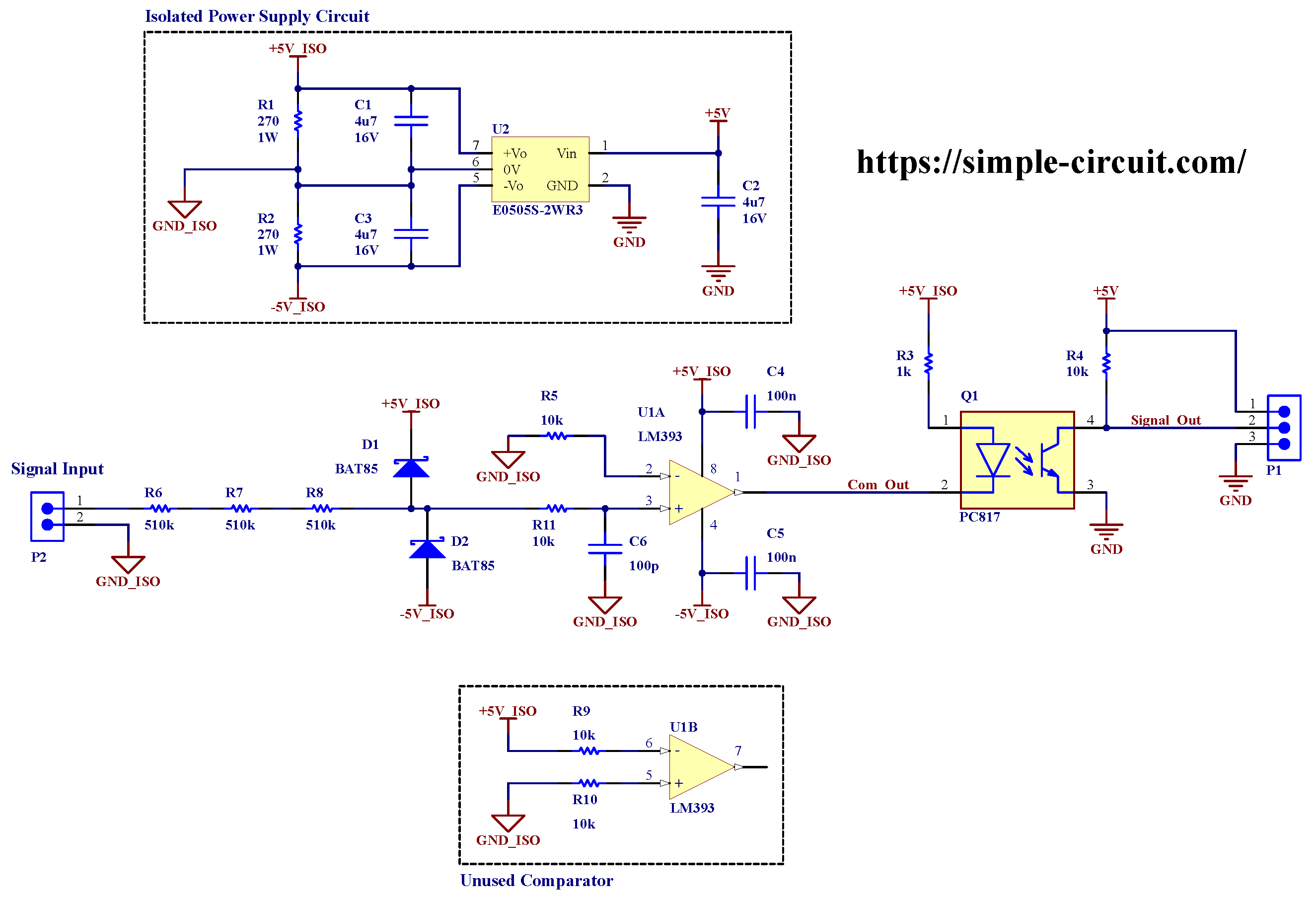
This post shows how to implement an isolated zero crossing detection circuit using an analog comparator and optocoupler, circuit schematic is the one below.
A part of this circuit may be subjected to high voltage which is very harmful to human body, be careful while trying to deal with high voltage circuits.
This project is provided with no warranty of any kind, DO IT AT YOUR OWN RISK!
Why Isolation?
Isolation between two circuits means preventing electric current (AC & DC) from flowing from one circuit to the other, while power and signal can still be able to transfer between the two circuits.
Isolation is used in a wide variety of applications and the most important factors are to protect human body and low voltage circuits from high voltage levels.
Hardware Required:
This is a list of the components used in this project.
- LM393 dual comparator (U1) —> datasheet
- PC817 optocoupler (or similar) (Q1) —> datasheet
- E0505S (or similar) dual output isolated DC/DC converter (U2) —> datasheet
- 2 x BAT85 small signal Schottky diode (D1, D2) —> datasheet
- 3 x 4.7 uF electrolytic capacitor (C1, C2, C3)
- 2 x 100 nF ceramic capacitor (C4, C5)
- 100 pF ceramic capacitor (C6)
- 2 x 270 ohm, 1 W resistor (R1, R2)
- 1k ohm resistor (R3)
- 5 x 10k ohm resistor (R4, R5, R9, R10, R11)
- 3 x 510k ohm resistor (R6, R7, R8)
Circuit Description:
The zero-crossing detection circuit designed in this project has an output isolated from the input. This means there is no direct physical contact between the input circuitry and the output circuitry.
The low voltage side is usually connected to a microprocessor circuit or a microcontroller based development board such as an Arduino platform. The Arduino board is directly connected to a PC or Laptop mainly for programming a monitoring purposes.
The high voltage side is connected to mains voltage to detect its zero crossing events. The human body must not directly get in touch with any of the mains terminals.
The isolated zero-crossing detection circuit proposed in this post uses an optocoupler (Q1) to isolate the signal that comes from the high voltage side and goes to the low voltage side.
The low voltage side as well as the high voltage side requires a power supply source to operate. The low voltage side is directly powered from the user power supply (for example a development board or power supply unit) with an input voltage of 5 Volts.
As shown in the circuit schematic, an isolated DC-to-DC converter with input of 5V and dual output of ±5V is used to provide an isolated power source to the high voltage side. In this example I used the part E0505S-2WR3 from MORNSUN, there are many equivalents to this part that can be replaced with.
The input of the isolated DC/DC converter is 5V where pin Vin (#1) is connected to circuit positive supply +5V, and pin GND (#2) is connected to circuit ground.
The output of the isolated DC/DC converter is +5V_ISO, GND_ISO, and -5V_ISO where pin +Vo (#7) is the positive output and pin -Vo (#5) is the negative output, both outputs are with respect to pin 0V (#6).
Optional – The used isolated DC/DC converter is a non regulated type and to get a nice output voltage the load should not be get less than 10%. For that, I connected a resistor of 270 Ohm to each output (R1, R2), total power absorbed by the two resistors is about 0.19W which is about the recommended 10%.
If the 1 Watt version is used then resistors R1 & R2 should be changed with higher resistances to minimize the converter output current (just keep it around the 10%).
The circuit shown above can detect zero-crossing events of domestic AC voltage levels, lets say up to 250 VAC. The input voltage is connected to P2 terminal (Signal Input).
Three through hole 1/4W resistors each of 510k Ohm (R6, R7, R8) are used to limit the current flowing to the circuit. A pair of Schottky diode (D1, D2) is used to clamp the input voltage to a safe level. The maximum voltage at the clamping diodes common point is 5V + VF and the minimum voltage is -5V -VF where VF is the forward voltage of the Schottky diode.
After clamping the input voltage using diodes D1 & D2, the signal is passed to the non-inverting input of the analog comparator (U1A) through 10k Ohm resistor (R11). Resistors: R6, R7, R8, R11 and capacitor C6 forms a low pass filter that helps eliminating some noise and also attenuating any harmonic with frequency higher than the cutoff frequency. Keep in mind that the low pass filter introduces some delay to the circuit.
The inverting terminal of the comparator is connected to the isolated, or high voltage ground (GND_ISO) through 10k resistor (R5).
One characteristic of the analog comparator is that it has a very low input current which means the current that flows through resistor R5 is very low and therefor the voltage across this resistor is very low (can be neglected).
Even the voltage across R5 resistor is neglected but the comparator inputs should not be connected directly to a low impedance point including circuit ground. Adding resistor to the input limits the current regardless of any fault condition.
The reference voltage of the comparator is zero volt since its inverting terminal is connected to ground (GND_ISO). This means the comparator output is the negative saturation voltage (-Vsat) whenever the input signal voltage is lower than the reference voltage (zero volt). This situation will illuminate the LED of the optocoupler (Q1) and a logic zero (zero volts) is sent to the isolated low voltage (control) circuit.
If the input signal voltage is positive then the comparator output will be floating (open collector output), the optocoupler’s LED will be off and a logic one (5 volts) is sent to the isolated low voltage (control) circuit.
A current limiting resistor of 1k (R3) is connected in series with the LED of the optocoupler. The optocoupler has also an open collector output, so a pull-up resistor of 10k (R4) is connected to the transistor collector terminal. Resistors R3 & R4 are chosen according the design requirements.
The LM393 comparator chip contains two independent comparators (2 channels), only one channel is used in this project. The unused comparator channel should be connected as shown in the circuit diagram. With this connection, the unused comparator does not affect the used one. The output of the unused comparator is left at a not connected situation.
Isolated Zero Crossing Detection Circuit – DIY PCB:
The following image shows a DIY PCB for the project. Most important components are highlighted, each with its part number.

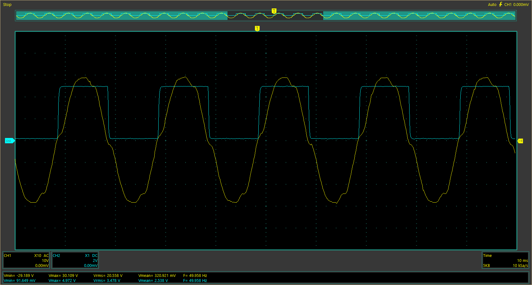
I made some real tests to the circuit, one of them is by connecting a step down transformer output to the input terminal of the circuit. The RMS output voltage of the used transformer is 20 VAC.
The image below shows a screen shoot from oscilloscope with channel 1 connected to the voltage input (yellow trace) and channel 2 is connected to the output of the circuit for capturing zero crossing events (blue color).
Please be careful while connecting the oscilloscope to the circuit, high voltage source should not directly connected to the oscilloscope even using X100 or X1000 probe, an isolation module (isolated probe) between the voltage source and the oscilloscope should be used.
Also, the circuit described in this post will loose its isolation property if an oscilloscope is connected to the input and the output at the same time without using an isolation probe. Oscilloscope usually share the same ground for all channels.
Reference:
Texas Instruments LM393 product page
Discover more from Simple Circuit
Subscribe to get the latest posts sent to your email.