This post shows how to configure and use Microchip PIC18F46K42 8-bit microcontroller integrated DMA (Direct Memory Access) module.
This example shows how to use the DMA module of the MCU to send screen data buffer to NOKIA 5110 LCD via SPI interface. The PIC compiler used in this example is CCS C.
The DMA controller allows data transfer between memory regions (GPR/SFR, PFM, EEPROM) directly without intervention from the CPU (Central Processing Unit), therefor the CPU can spend more time on other tasks.
The PIC18F46K42 microcontroller has two independent DMA modules, in this project one DMA module is used to transfer display data buffer which is stored in MCU GPR (General Purpose Register) to SPI (Serial Peripheral Interface) module transmit buffer SFR (Special Function Register).
The name Nokia 5110 (3310) LCD comes from Nokia 5110 (or Nokia 3310) mobile phone. The Nokia 5110 LCD contains the PCD8544 controller, it is similar to the one used in Nokia 5110 mobile phone, it uses SPI interface protocol with maximum clock frequency of 4 MHz, it requires 5 control pins (at most), it’s low cost and easy to use.
The resolution of this LCD is 84 x 48 which means it has 4032 pixels. This module works with 3.3V only and it doesn’t support 5V (not 5V tolerant), this means interfacing it with 5V microcontroller such as PIC18F46K42 MCU requires voltage level shifter.
The Nokia 5110 LCD screen is shown below:
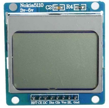
This module has 8 pins (from left to right): RST (reset), CE (chip enable), DC (or D/C: data/command), Din (data in), Clk (clock), VCC (3.3V), BL (back light) and Gnd (ground).
The pins which should be connected to the microcontroller are: RST, CE, DC, Din and Clk.
Hardware Required:
- PIC18F46K42 microcontroller —-> datasheet
- Nokia 5110 (3310) LCD module
- AMS1117-3V3 voltage regulator
- 22 uF capacitor
- 10 uF capacitor
- 3 x 100 nF ceramic capacitor
- 5 x 2k resistor
- 5 x 1 resistor
- 5V source
- Breadboard
- Jumper wires
- PIC programmer (PICkit 3, PICkit 4…)
Interfacing PIC18F46K42 MCU with Nokia 5110 LCD circuit:
The following image shows example simplified circuit schematic diagram (click on the image for better view)..
The Nokia 5110 which is shown in the circuit diagram has 8 pins (from left to right): RST (reset), CE (chip enable), DC (or D/C: data/command), Din (data in), Clk (clock), VCC (3.3V), BL (back light) and Gnd (ground).
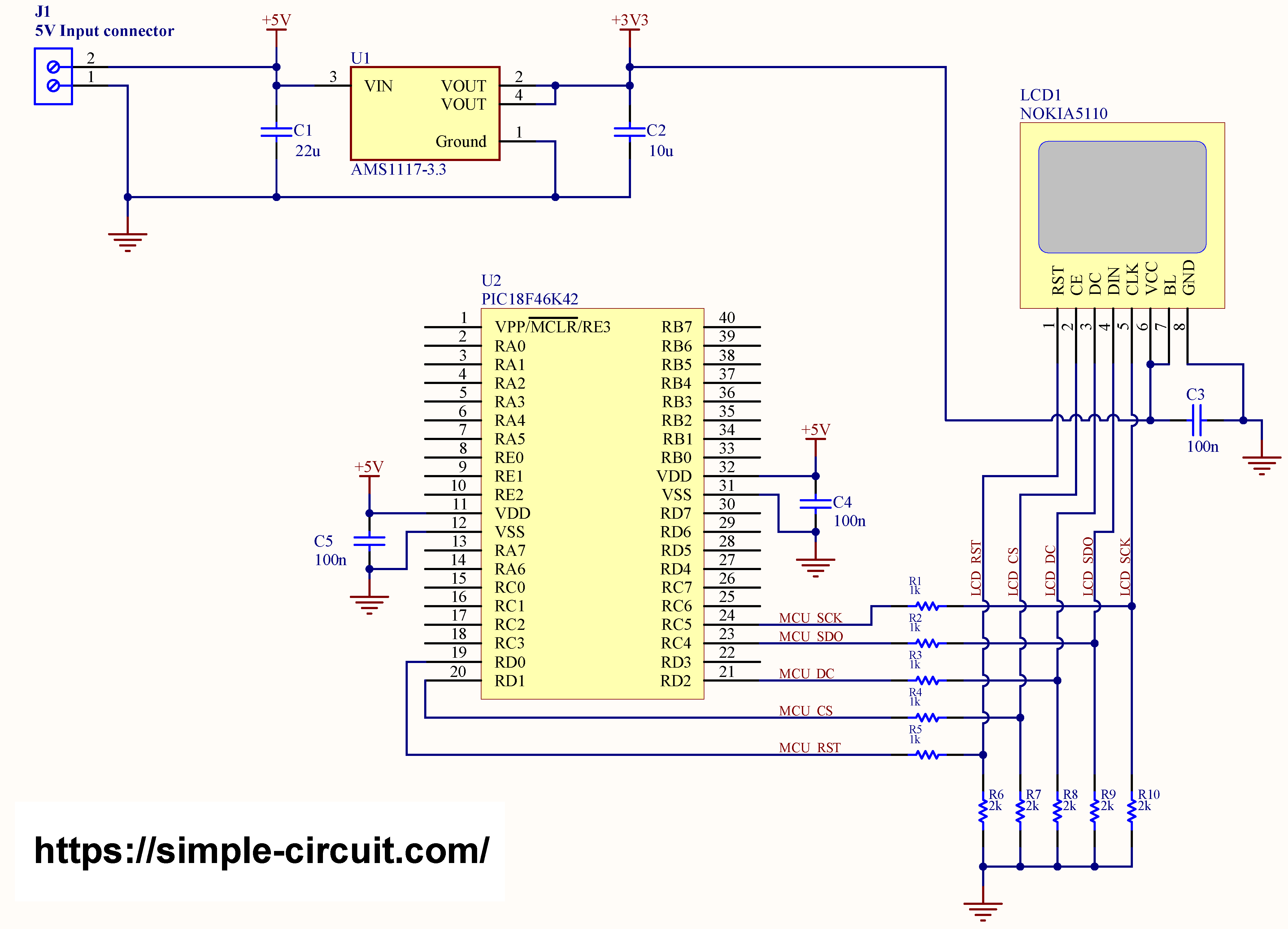
The main power source voltage of the circuit is 5V, it’s connected to connector J1 (5V Input connector) where pin 1 is negative and pin 2 is positive.
The Nokia 5110 LCD works with 3.3V only (power supply and control lines). The LCD module is supplied with 3.3V from the AMS1117-3V3 voltage regulator (U1) output, this regulator converts 5V input into 3.3V (supplies the LCD controller PCD8544 with regulated 3V3).
All PIC18F46K42 microcontroller output pins are 5V, connecting a 5V pin directly to the Nokia 5110 LCD may damage its controller.
To connect the PIC18F46K42 to the LCD module, I used voltage divider for each line. This means there are 5 voltage dividers, each one consists of 1k and 2k resistors, this drops control voltage from 5V into 3.3V.
Actually, choosing the values of voltage divider resistors depends on many factors such as: maximum frequency, pin capacitance … but 1k & 2k will do the job as it should be, however, using a 3.3V microcontroller is recommended when dealing with 3.3V devices.
So, the Nokia 5110 LCD pins are connected to PIC18F46K42 MCU as follows (each one through voltage divider):
RST (reset) pin is connected to pin RD0 (#19),
CE (chip enable) pin is connected to pin RD1 (#20),
DC (data/command) pin is connected to pin RD2 (#21),
DIN (data in) pin is connected to pin RC4 (#23),
CLK (clock) pin is connected to pin RC5 (#24).
VCC and BL are connected to AMS1117-3V3 regulator output pin and GND is connected to circuit ground (0V).
In this project the PIC18F46K42 microcontroller runs with its internal oscillator @ 16 MHz, MCLR pin is configured as an input pin.
Interfacing PIC18F46K42 MCU with Nokia 5110 LCD using DMA controller C code:
The following C code is for CCS C compiler, it was tested with versions 5.104.
To be able to compile project C code with no error, 2 libraries are required:
The first library is a driver for the Nokia 5110 LCD (PCD8544 controller), its full name (with extension) is PCD8544.c, download link is below:
Nokia 5110 LCD library for CCS C compiler
The second library is graphics library, its full name is GFX_Library.c, download link is the one below:
Graphics library for CCS C compiler
after the download of the 2 libraries, add both files to project folder.
Hints:
The 2 library files are included in the main code as shown below:
1 2 | #include <PCD8544.c> // include PCD8544 controller driver source code (Nokia 5110 LCD driver) #include <GFX_Library.c> // include graphics library source code |
Connection of LCD pins with the microcontroller are defined as:
1 2 3 4 5 6 | // define Nokia 5110 LCD module pin connections #define LCD_RST PIN_D0 // reset pin, optional! #define LCD_CS PIN_D1 // chip select pin #define LCD_DC PIN_D2 // data/command pin #define LCD_DAT PIN_C4 // data-in pin (MOSI) #define LCD_CLK PIN_C5 // clock pin |
The PIC18F46K42 DMA module is initialized using the function DMA_Initialize(), and the LCD is updated (refreshed) whenever the function DMA_Transfer() is called. Calling the last function starts sending the data buffer pcd8544_buffer to the display using DMA module by setting the bit: SIRQEN, when all data are transferred this bit is cleared. Once data transfer is completed, DMA1 Interrupt is called and the LCD is de-selected by rising the CS pin (RD1).
Note that CCS C compiler already has functions that can initialize the DMA module and content of the function DMA_Initialize() can be replaced by the following:
1 2 3 | setup_dma(1, DMA_TRIGGER_SPI1TX, DMA_TRIGGER_NONE); dma_start(1, DMA_SOURCE_ADDR_IS_SFR_GPR | DMA_ONE_SHOT_FROM_SOURCE_COUNT | DMA_INC_SOURCE_ADDR | DMA_DEST_ADDR_UNCHANGED | DMA_SW_TRIGGER_STARTS_XFER, getenv("SFR:SPI1TXB"), &pcd8544_buffer[0], 1, 504); |
Instead of CCS C compiler above functions I used to set manually each DMA register because its more easier to relate the settings with device’s datasheet.
The DMA module is configured such as source start address is the address of pcd8544_buffer[0] and destination start address is SPI1 module transmit buffer register SPI1TXB.
The source start address has to be incremented after each transfer in order to transfer all bytes located in the pcd8544_buffer array. In the other hand the destination address remains unchanged after each transfer as we want to transfer all data through the same SPI module.
After each transfer, SPI1TXB interrupt triggers the DMA controller for another byte transfer until the whole data buffer pcd8544_buffer transfer is completed, the size of the data buffer is 504 bytes. Data transfer is initialized by setting the bit SIRQEN and is automatically cleared once all data transfer complete.
Rest of code is described through comments.
Full CCS C code:
1 2 3 4 5 6 7 8 9 10 11 12 13 14 15 16 17 18 19 20 21 22 23 24 25 26 27 28 29 30 31 32 33 34 35 36 37 38 39 40 41 42 43 44 45 46 47 48 49 50 51 52 53 54 55 56 57 58 59 60 61 62 63 64 65 66 67 68 69 70 71 72 73 74 75 76 77 78 79 80 81 82 83 84 85 86 87 88 89 90 91 92 93 94 95 96 97 98 99 100 101 102 103 104 105 106 107 108 109 110 111 112 113 114 115 116 117 118 119 120 121 122 123 124 125 126 127 128 129 130 131 132 133 134 135 136 137 138 139 140 141 142 143 144 145 146 147 148 149 150 151 152 153 154 155 156 157 158 159 160 161 162 163 164 165 166 167 168 169 170 171 172 173 174 175 176 177 178 179 180 181 182 183 184 185 186 187 188 189 190 191 192 193 194 195 196 197 198 199 200 201 202 203 204 205 206 207 208 209 210 211 212 213 214 215 216 217 218 219 220 221 222 223 224 225 226 227 228 229 230 231 232 233 234 235 236 237 238 239 240 241 242 243 244 245 246 247 248 249 250 251 252 253 254 255 256 257 258 259 260 261 262 263 264 265 266 267 268 269 270 271 272 273 274 275 276 277 278 279 280 281 282 283 284 285 286 287 288 289 290 291 292 293 294 295 296 297 298 299 300 301 302 303 304 305 306 307 308 309 310 311 312 313 314 315 316 317 318 319 320 321 322 323 324 325 326 327 328 329 330 331 332 333 334 335 336 337 338 339 340 341 342 343 344 345 346 347 348 349 350 351 352 353 354 355 356 357 358 359 360 361 362 363 364 365 366 367 368 369 370 371 372 373 374 375 376 377 378 379 380 381 382 383 384 385 386 387 388 389 390 391 392 393 394 395 396 397 398 399 400 401 402 403 404 405 406 407 408 409 410 411 412 413 414 415 416 417 418 419 420 421 422 423 424 425 426 427 428 429 430 431 432 433 434 435 436 437 438 439 440 441 442 443 444 445 446 447 448 449 450 451 452 453 454 455 | /***************************************************************************** Interfacing PIC18F46K42 microcontroller with Nokia 5110 (3310) LCD display. DMA Module of the MCU is used to transfer data buffer to the SPI display. C Code for CCS C compiler. This is a free software with NO WARRANTY. https://simple-circuit.com/ /***************************************************************************** This is an example sketch for our Monochrome Nokia 5110 LCD Displays Pick one up today in the adafruit shop! ------> http://www.adafruit.com/products/338 These displays use SPI to communicate, 4 or 5 pins are required to interface Adafruit invests time and resources providing this open source code, please support Adafruit and open-source hardware by purchasing products from Adafruit! Written by Limor Fried/Ladyada for Adafruit Industries. BSD license, check license.txt for more information All text above, and the splash screen must be included in any redistribution *********************************************************************/ // define Nokia 5110 LCD module pin connections #define LCD_RST PIN_D0 // reset pin, optional! #define LCD_CS PIN_D1 // chip select pin #define LCD_DC PIN_D2 // data/command pin #define LCD_DAT PIN_C4 // data-in pin (MOSI) #define LCD_CLK PIN_C5 // clock pin #define PCD8544_SPI_Write(x) SPI_WRITE(x) #include <18F46K42.h> #FUSES NOWDT,NOMCLR,PUT_64MS,NOLVP #use delay(internal = 16MHz) // SPI module SCK & SDO pin definition #pin_select SCK1 = LCD_CLK #pin_select SDO1 = LCD_DAT #include <PCD8544.c> // include PCD8544 controller driver source code (Nokia 5110 LCD driver) #include <GFX_Library.c> // include graphics library source code // register definition #byte SPI1TXB = getenv("SFR:SPI1TXB") // SPI transmit buffer register #byte DMA1CON0 = getenv("SFR:DMA1CON0") // DMA1 control register 0 #byte DMA1CON1 = getenv("SFR:DMA1CON1") // DMA1 control register 1 #byte DMA1SSAU = getenv("SFR:DMA1SSAU") // DMA1 source start address upper register #byte DMA1SSAH = getenv("SFR:DMA1SSAH") // DMA1 source start address high register #byte DMA1SSAL = getenv("SFR:DMA1SSAL") // DMA1 source start address low register #byte DMA1SSZH = getenv("SFR:DMA1SSZH") // DMA1 source size high register #byte DMA1SSZL = getenv("SFR:DMA1SSZL") // DMA1 source size low register #byte DMA1DSAH = getenv("SFR:DMA1DSAH") // DMA1 destination start address high register #byte DMA1DSAL = getenv("SFR:DMA1DSAL") // DMA1 destination start address low register #byte DMA1DSZH = getenv("SFR:DMA1DSZH") // DMA1 destination size high register #byte DMA1DSZL = getenv("SFR:DMA1DSZL") // DMA1 destination size low register #byte DMA1SIRQ = getenv("SFR:DMA1SIRQ") // DMA1 start interrupt request source selection register #byte PRLOCK = getenv("SFR:PRLOCK") // priority lock register #bit PRLOCKED = PRLOCK.0 // PR register lock bit #bit SIRQEN = DMA1CON0.6 // start of transfer interrupt request enable bit // end register definition // define random max number #define RAND_MAX (display_width - 1) // include std library source code (required by rand() function) #include <stdlib.h> #define NUMFLAKES 10 #define XPOS 0 #define YPOS 1 #define DELTAY 2 #define LOGO16_GLCD_HEIGHT 16 #define LOGO16_GLCD_WIDTH 16 rom char logo16_glcd_bmp[] = { 0b00000000, 0b11000000, 0b00000001, 0b11000000, 0b00000001, 0b11000000, 0b00000011, 0b11100000, 0b11110011, 0b11100000, 0b11111110, 0b11111000, 0b01111110, 0b11111111, 0b00110011, 0b10011111, 0b00011111, 0b11111100, 0b00001101, 0b01110000, 0b00011011, 0b10100000, 0b00111111, 0b11100000, 0b00111111, 0b11110000, 0b01111100, 0b11110000, 0b01110000, 0b01110000, 0b00000000, 0b00110000 }; // select the LCD and start DMA transfer void DMA_Transfer() { output_low(LCD_DC); output_low(LCD_CS); PCD8544_SPI_Write(LCD_SETYADDR); PCD8544_SPI_Write(LCD_SETXADDR); output_high(LCD_DC); SIRQEN = 1; // wait for data transfer to complete while (SIRQEN) ; } void testdrawbitmap(rom uint8_t *bitmap, uint8_t w, uint8_t h) { static uint8_t icons[NUMFLAKES][3], f, x_pos, y_pos; // initialize for (f=0; f< NUMFLAKES; f++) { icons[f][XPOS] = rand(); icons[f][YPOS] = 0; icons[f][DELTAY] = (rand() % 5) + 1; } icons[0][XPOS] = 30; while (TRUE) { uint8_t f; // draw each icon for (f=0; f< NUMFLAKES; f++) { x_pos = icons[f][XPOS]; y_pos = icons[f][YPOS]; display_drawBitmapV2(x_pos, y_pos, bitmap, w, h, BLACK); } // print data on LCD DMA_Transfer(); delay_ms(200); // then erase it + move it for (f=0; f< NUMFLAKES; f++) { x_pos = icons[f][XPOS]; y_pos = icons[f][YPOS]; display_drawBitmapV2(x_pos, y_pos, bitmap, w, h, WHITE); // move it icons[f][YPOS] += icons[f][DELTAY]; // if its gone, reinit if (icons[f][YPOS] > display_height) { icons[f][XPOS] = rand(); icons[f][YPOS] = 0; icons[f][DELTAY] = (rand() % 5) + 1; } } } } void testdrawchar(void) { display_setTextSize(1); display_setTextColor(BLACK); display_setCursor(0, 0); for (uint8_t i=0; i < 168; i++) { if (i == '\n' || i == '\r') continue; display_print(i); } // print data on LCD DMA_Transfer(); } void testdrawcircle(void) { for (int16_t i=0; i<display_height; i+=2) { display_drawCircle(display_width/2, display_height/2, i, BLACK); // print data on LCD DMA_Transfer(); } } void testfillrect(void) { uint8_t color = 1; for (int16_t i=0; i<display_height/2; i+=3) { // alternate colors display_fillRect(i, i, display_width-i*2, display_height-i*2, color%2); // print data on LCD DMA_Transfer(); color++; } } void testdrawtriangle(void) { for (int16_t i=0; i<min(display_width,display_height)/2; i+=5) { display_drawTriangle(display_width/2, display_height/2-i, display_width/2-i, display_height/2+i, display_width/2+i, display_height/2+i, BLACK); // print data on LCD DMA_Transfer(); } } void testfilltriangle(void) { uint8_t color = BLACK; for (int16_t i=min(display_width,display_height)/2; i>0; i-=5) { display_fillTriangle(display_width/2, display_height/2-i, display_width/2-i, display_height/2+i, display_width/2+i, display_height/2+i, color); if (color == WHITE) color = BLACK; else color = WHITE; // print data on LCD DMA_Transfer(); } } void testdrawroundrect(void) { for (int16_t i=0; i<display_height/2-2; i+=2) { display_drawRoundRect(i, i, display_width-2*i, display_height-2*i, display_height/4, BLACK); // print data on LCD DMA_Transfer(); } } void testfillroundrect(void) { uint8_t color = BLACK; for (int16_t i=0; i<display_height/2-2; i+=2) { display_fillRoundRect(i, i, display_width-2*i, display_height-2*i, display_height/4, color); if (color == WHITE) color = BLACK; else color = WHITE; // print data on LCD DMA_Transfer(); } } void testdrawrect(void) { for (int16_t i=0; i<display_height/2; i+=2) { display_drawRect(i, i, display_width-2*i, display_height-2*i, BLACK); // print data on LCD DMA_Transfer(); } } void testdrawline() { int16_t i; for (i=0; i<display_width; i+=4) { display_drawLine(0, 0, i, display_height-1, BLACK); // print data on LCD DMA_Transfer(); } for (i=0; i<display_height; i+=4) { display_drawLine(0, 0, display_width-1, i, BLACK); // print data on LCD DMA_Transfer(); } delay_ms(250); display_clear(); for (i=0; i<display_width; i+=4) { display_drawLine(0, display_height-1, i, 0, BLACK); // print data on LCD DMA_Transfer(); } for (i=display_height-1; i>=0; i-=4) { display_drawLine(0, display_height-1, display_width-1, i, BLACK); // print data on LCD DMA_Transfer(); } delay_ms(250); display_clear(); for (i=display_width-1; i>=0; i-=4) { display_drawLine(display_width-1, display_height-1, i, 0, BLACK); // print data on LCD DMA_Transfer(); } for (i=display_height-1; i>=0; i-=4) { display_drawLine(display_width-1, display_height-1, 0, i, BLACK); // print data on LCD DMA_Transfer(); } delay_ms(250); display_clear(); for (i=0; i<display_height; i+=4) { display_drawLine(display_width-1, 0, 0, i, BLACK); // print data on LCD DMA_Transfer(); } for (i=0; i<display_width; i+=4) { display_drawLine(display_width-1, 0, i, display_height-1, BLACK); // print data on LCD DMA_Transfer(); } delay_ms(250); } // DMA1 source count ISR #INT_DMA1SCNT void DMA_ISR(void) { // deselect the LCD output_high(LCD_CS); } // DMA module initialization void DMA_Initialize() { uint32_t source_addr = &pcd8544_buffer[0]; // source address uint16_t source_size = 504; // source size // DMA1CON1 register setting: //-destination address remains unchanged after each transfer completion //-source memory points to SFR/GPR //-source address is incremented after each transfer completion //-SIRQEN bit is cleared when Source Counter reloads DMA1CON1 = 0x03; // source size DMA1SSZH = (source_size >> 8); DMA1SSZL = source_size; // source start address DMA1SSAU = (source_addr >> 16); DMA1SSAH = (source_addr >> 8); DMA1SSAL = source_addr; // destination size DMA1DSZH = 0x00; DMA1DSZL = 0x01; // destination start address, 0x3D11 (SPI1TXB) DMA1DSAH = 0x3D; DMA1DSAL = 0x11; // start trigger source SPI1TXB (0x15) DMA1SIRQ = 0x15; // set PRLOCKED bit to grant memory access to DMA disable_interrupts(GLOBAL); PRLOCK = 0x55; PRLOCK = 0xAA; PRLOCKED = 1; enable_interrupts(GLOBAL); // enable DMA module DMA1CON0 = 0x80; } // main function void main() { delay_ms(500); // initialize SPI module in master mode with CLK freq = 4 MHz setup_spi( SPI_MASTER | SPI_XMIT_L_TO_H | SPI_TX_ONLY_MODE | SPI_SCK_IDLE_LOW, 4000000 ); // DMA module initialization DMA_Initialize(); // enable DMA1 source counter interrupt enable_interrupts(INT_DMA1SCNT); // initialize the LCD LCD_begin(); // init done // you can change the contrast around (0 ... 63) to //adapt the display for the best viewing! display_setContrast(60); // print data on LCD //DMA_Transfer(); // show splashscreen display(); delay_ms(2000); display_clear(); // clears the screen and buffer // draw a single pixel display_drawPixel(10, 10, BLACK); display(); delay_ms(2000); display_clear(); // draw many lines testdrawline(); display(); delay_ms(2000); display_clear(); // draw rectangles testdrawrect(); display(); delay_ms(2000); display_clear(); // draw multiple rectangles testfillrect(); display(); delay_ms(2000); display_clear(); // draw mulitple circles testdrawcircle(); display(); delay_ms(2000); display_clear(); // draw a circle, 10 pixel radius display_fillCircle(display_width/2, display_height/2, 10, BLACK); display(); delay_ms(2000); display_clear(); testdrawroundrect(); delay_ms(2000); display_clear(); testfillroundrect(); delay_ms(2000); display_clear(); testdrawtriangle(); delay_ms(2000); display_clear(); testfilltriangle(); delay_ms(2000); display_clear(); // draw the first ~12 characters in the font testdrawchar(); display(); delay_ms(2000); display_clear(); // text display tests display_setTextSize(1); display_setTextColor(BLACK); display_setCursor(0, 0); display_print("Hello, world!\r\n"); display_setTextColor(WHITE, BLACK); // 'inverted' text printf(display_print, "%f\r\n", 3.141592); display_setTextSize(2); display_setTextColor(BLACK); printf(display_print, "0x%LX\r\n", 0xDEADBEEF); // print data on LCD DMA_Transfer(); delay_ms(2000); // rotation example display_clear(); display_setRotation(1); // rotate 90 degrees counter clockwise, can also use values of 2 and 3 to go further. display_setTextSize(1); display_setTextColor(BLACK); display_setCursor(0, 0); display_print("Rotation\r\n"); display_setTextSize(2); display_print("Example!\r\n"); // print data on LCD DMA_Transfer(); delay_ms(2000); // revert back to no rotation display_setRotation(0); // miniature bitmap display display_clear(); display_drawBitmapV2(30, 16, logo16_glcd_bmp, 16, 16, BLACK); // print data on LCD DMA_Transfer(); // invert the display display_invert(true); delay_ms(1000); display_invert(false); delay_ms(1000); // draw a bitmap icon and 'animate' movement testdrawbitmap(logo16_glcd_bmp, LOGO16_GLCD_WIDTH, LOGO16_GLCD_HEIGHT); } // end of code. |
The following short video shows my DIY circuit :
Discover more from Simple Circuit
Subscribe to get the latest posts sent to your email.